1) EO polymer refilled slot PCW modulator
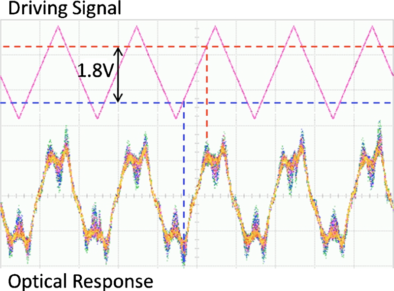
Fig. 1 shows the schematic of the EO polymer refilled slot PCW, and the corresponding simulations showing the effect of applied voltage across the slot on the dispersion diagram. Due to large change produced, a very low power modulator can be developed. Fabricated structure and testing results are shown in Fig. 2. We have achieved 735pm=V effective in-device r33 and 0.44Vmm VπL, all of which are the best results that have ever been reported, to our knowledge
(a) 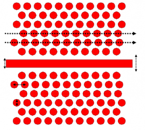 |
(b) 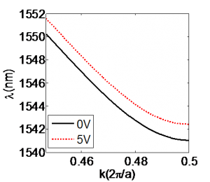 |
(c) 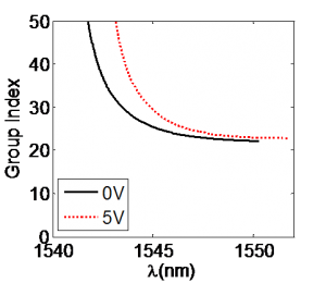 |
2) p-i-n modulator utilizing slow light photonic crystal waveguides.
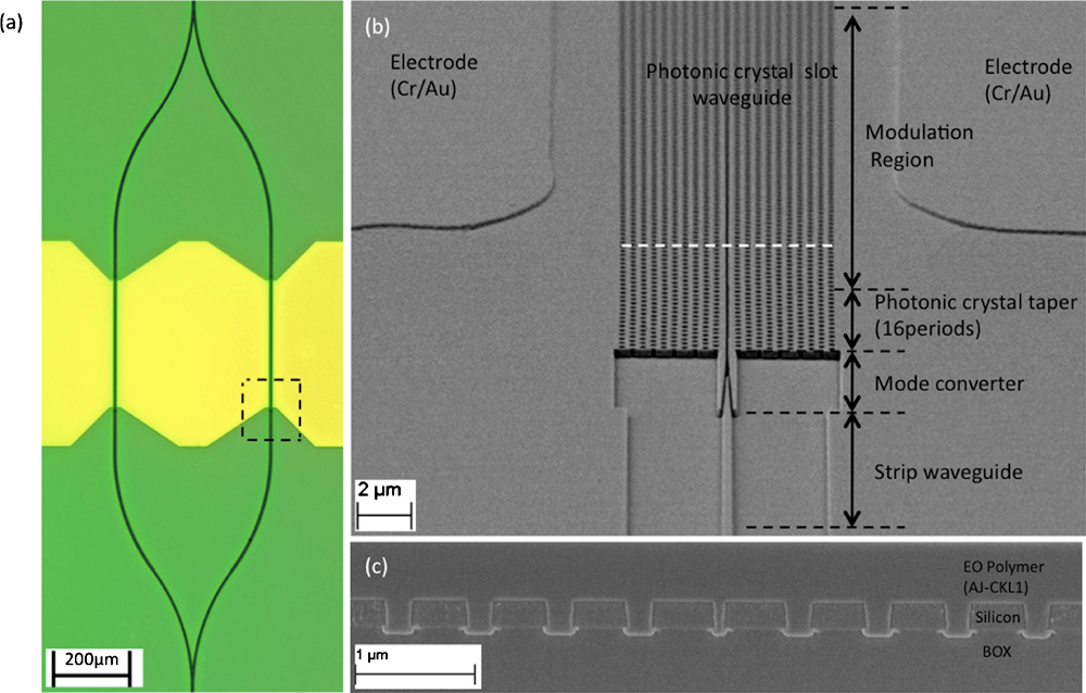
We previously demonstrated a 80µm long interaction length modulator based on photonic crystal waveguide. By engineering the band structure of the PCW, higher and flatter group index over a broad bandwidth is possible. Group index ng=26.7 ± 10% over a bandwidth of 18 nm (1539 nm~1557 nm), corresponding to delay–normalized bandwidth product of ng(∆ω/ω)=0.31, is achieved. Fig. 3 shows the schematic of the modulator structure and SEM images of the fabricated structure. The operation of the device is shown in Fig. 4. A large signal operation with a record low maximum Vπ×L of 0.0464 V⋅mm over the low-dispersion optical spectral range is achieved.
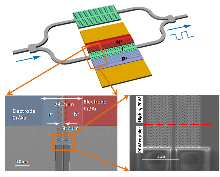
Fig. 3. A schematic of photonic crystal MZI modulator; scanning electronic microscope images of the active arm of the modulator and the photonic crystal waveguide coupler are shown as insets.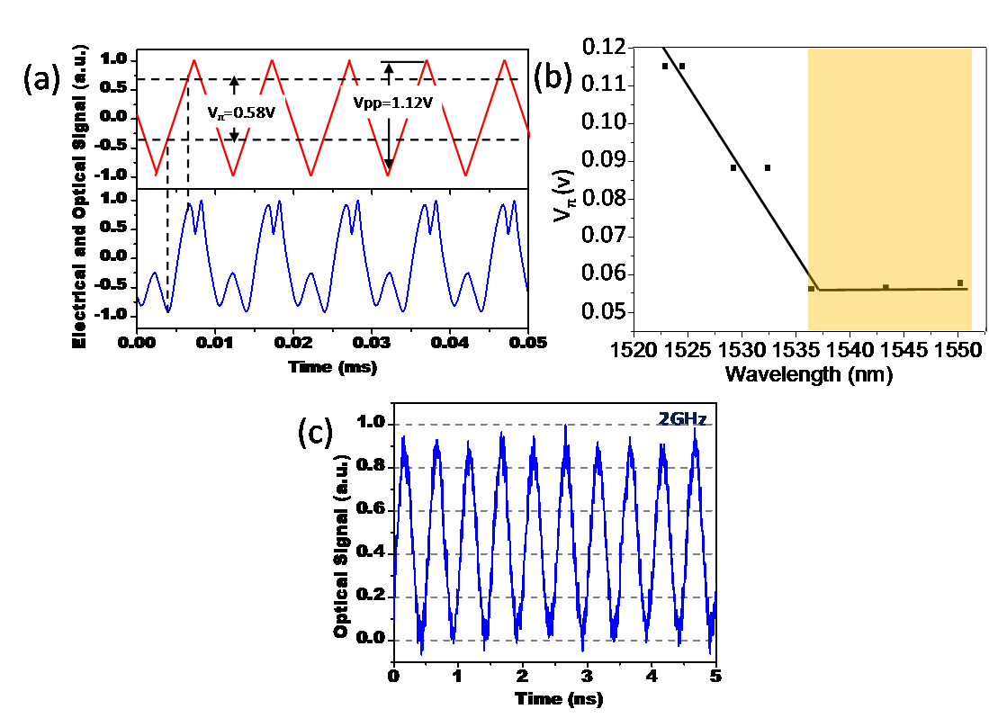
3) Silicon Nanomembrane
Silicon nanomembranes (SiNMs) are very thin sheets of silicon that have been released from silicon-on-insulator (SOI) wafers and re-deposited on other rigid or flexible hosts. Silicon nanomembranes (SiNMs) are processable like bulk Si and retain the electronic and optical properties of bulk Si. However, due to their thinness, their mechanical properties are interestingly different compared to bulk Si. Thus, all kinds of Si devices can potentially be fabricated, and high-volume manufacturing is feasible, thus utilizing and integrating the best features from different material systems.
We have developed SiNM transfer methods based on stamp printing, modified stamp printing and bonding techniques. Using such techniques, unique SiNM devices such as optical waveguides, photonic crystal waveguides, multimode interference couplers (MMI) etc, as well as extremely delicate structures such as EO polymer refilled slot photonic crystal waveguide modulators, p-i-n modulators etc have been developed on unusual substrates such as glass, polyimide etc.
The program is currently supported by a SBIR grant from the Air Force Office of Scientif Research (AFOSR)
4) DENSE WAVELENGTH DIVISION MULTIPLEXING (DWDM)
Wavelength division multiplexing (WDM) and demultiplexing (WDDM) devices are considered to be two of the key elements for enhancing the transmission bandwidth of optical communications and sensor systems. During the past 20 years, various types of WDMs and WDDMs have been proposed and demonstrated. Wavelength-division multiplexing (WDM) technology allows multiple optical channels to be simultaneously transmitted at different wavelengths through a single optical fiber, and is a useful means of making full use of the low-loss characteristics of optical fibers over a wide-wavelength region.
Besides its capability to efficiently exploit the huge bandwidth of single mode optical fibers, WDM is promising for constructing different levels of transparency to optical transmissions (i.e., independent of data bit-rate, modulation format, or protocol), which permits excellent upgrading and backward compatibility of the current networks. This makes WDM the key technology for tomorrow’s developments in data, voice, imaging, and video communications.
The program was supported by a SBIR grant from the Department of Defense